 |
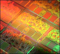
| Source: Intel |
Chip manufacturers are in a race to the bottom in terms of die size, and while this kind of one-upsmanship is good for fostering competition, it may prove unsustainable, industry-watchers say.
Intel (NASDAQ: INTC) has led the way last year with its move to 32 nanometers (NM) later this year, and is now targeting 28nm. IBM and its Technology Alliance, which includes partners like ST Microelectronics, AMD/Global Foundries, Samsung, and Chartered Semiconductor, have been at 45nm and planned to move to 32nm later this year.
Also, AMD’s (NYSE: AMD) Globalfoundry business announced its own plans to move to 32nm independent of the alliance. AMD spun off its foundry business as a separate, stand-alone company earlier this year. It had been at 45nm as well for the latest generation of AMD processors.
IBM is planning low-power 28nm processors for power-sensitive markets, like handheld devices. Because it uses High K Metal Gate technology, there is considerably less power leakage, which means less power loss and less heat. Early production is anticipated in the second half of 2010 but clients can begin their 32nm to 28nm migration planning already with early test kits.
“Through this collaboration, IBM and its alliance partners are helping to accelerate development of next-generation technology to achieve high-performance, energy-efficient chips at the 28nm process level, maintaining our focus on technology leadership for our clients and partners,” said Gary Patton, vice president for IBM’s Semiconductor Research and Development Center in a statement.
AMD has announced plans for a 32nm CPU, codenamed “Liano,” in 2011. The company said its Globalfoundries manufacturing arm is on track to manufacture 32nm semiconductors in the first half of 2010 and will begin accepting half-node 28nm designs in the second half of that year.
For technology buyers, there are some important implications: Smaller chips mean they are slightly faster and require less power. The use of High K Metal Gate means less leakage, good for power and cooling.
But this race to become the smallest mostly benefits IBM and AMD, said Jim McGregor, senior analyst with In-Stat.
“It’s gotten to the point that process technology and manufacturing is very expensive, and there’s no guarantee it’s going to work flawlessly,” he told InternetNews.com. “It’s to the point where it’s a risky proposition to go to a new process node, and it’s an expensive process for foundry companies. They are trying to lock in customers for the future, saying we’re going to be here at a certain point.”
There are numerous semiconductor makers that don’t make their own processors, like graphics giant nVidia. They often stick with a process and optimize for it and then skip a few generations because moving from one design process to another is expensive and they get little to no return on investment.
“TSMC and other fab companies have had a real trouble pushing customers to latest process because they didn’t see the value associated with the cost of the move,” he said. “At least with 32nm, IBM could say they have High K Metal Gate.”
The move to a smaller process designs is good for smartphones and mobile Internet devices.
“They’re adding high-performance screens, they want to add accelerometers for motion detection and high definition output, and all while increasing battery life,” McGregor said. “A smaller process node is smaller footprint and lower power draw and hopefully means longer battery life.”


